Ad9361 dac sub (ad9361_dac_sub)
Design
The AD9361 DAC Sub is a subdevice worker whose primary purpose is to time-interleave data streams for two TX channels in preparation for sending to the AD9361 IC pins (independent of which of the IC’s P0/P1 buses the TX data streams are sent to). Time-interleaving occurs according to the timing diagrams specified in AD9361_Reference_Manual_UG-570.pdf. This worker ingests data from at most two instances of the ad9361_dac.hdl device worker, each which handles a single TX channel data stream, and time-interleaves all channels onto a single data bus that is sent out eventually (via devsignals to Ad9361 data sub (ad9361_data_sub)) to the appropriate TX data stream pins of the AD9361 IC.
A block diagram representation of the implementation is given in Figure 183:
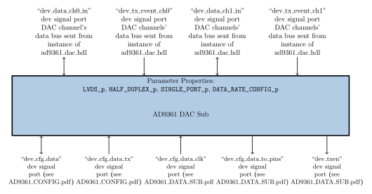
Figure 183: ad9361_dac_sub block diagram.
Interface
<HdlDevice language='vhdl' libraries='util ocpi.core.bsv'
  ExactParts="
    zynq:xc7z020-1-clg484
    zynq_ise:xc7z020_ise_alias-1-clg484
    zynq_ultra:xczu7ev-2-ffvc1156e
    virtex6:xc6vlx240t-1-ff1156
    stratix4:ep4sgx230k-c2-f40
    artix7:xc7a50t-2-csg325"
  OnlyTargets="zynq zynq_ise virtex6 isim xsim"
  SourceFiles="
    event_in_x2_to_txen.vhd
    ad936x_tx_data_cmos_single_port_fdd_ddr.vhd
    ad9361_dac_sub_cmos_single_port_fdd_ddr.vhd">

  <!-- By design, this worker provides control and/or data plane functionality
       that is never intended to be exposed by any other worker. Accordingly,
       this worker defines the ComponentSpec element inside this OWD file, as
       opposed to creating an OCS file including said functionality which could
       be used by other workers. -->
  <ComponentSpec nocontrol="true"/>

  <!-- Parameters -->

  <!-- This parameter property corresponds to the "LVDS Mode" bit 4 in the parallel port configuration 3
       register at 0x012. -->
  <Property name='LVDS_p' type='bool' parameter='true' default='false'
            description='Use LVDS TX data bus interleaving scheme, otherwise use CMOS interleaving scheme.
                         Default is CMOS.'/>
  <!-- This parameter property corresponds to the "Half Duplex Mode" bit 3 in the parallel port
       configuration 3 register 0x12 -->
  <Property name='HALF_DUPLEX_p' type='bool' parameter='true' default='false'
            description='Use half duplex mode, otherwise use full duplex mode. Must be false when using LVDS mode.'/> <!-- TODO / FIXME support runtime_dynamic enumeration? -->
  <!-- This parameter property corresponds to the "Single Port Mode" bit 2 in the parallel port
       configuration 3 register 0x12 -->
  <Property name='SINGLE_PORT_p' type='bool' parameter='true' default='false'
            description='Use single port, otherwise use both (dual) ports.  Default is to use both ports. Must be false when using LVDS mode.'/>
  <!-- This parameter property corresponds to the "Single Data Rate" bit 5 in the parallel port
       configuration 3 register 0x12 -->
  <Property name='DATA_RATE_CONFIG_p' type='enum' enums='SDR,DDR'
                                      parameter='true'
                                      default='DDR'
                                      description='This should have a value of DDR when LVDS_p has a value of true. Either value is acceptable when LVDS_p has a value of false (i.e. CMOS mode is used).'/>

  <!-- Dev Signal Ports -->

  <devsignal name='dev_cfg_data'     signals='ad9361-cfg-data-signals.xml'    master='true'/>
  <devsignal name='dev_cfg_data_tx'  signals='ad9361-cfg-data-tx-signals.xml' master='true'/>
  <devsignal name='dev_data_clk'     signals='ad9361-data-clk-signals.xml'    master='true'/>
  <devsignal name='dev_data_to_pins' signals='ad9361-data-dac-signals.xml'    master='true'/>
  <devsignal name='dev_txen'     signals='txen-out-signals.xml'           master='true'/>

  <!-- to supported ad9361_dac.hdl -->
  <devsignal name='dev_data_ch0_in' signals='dac-12-signals.xml'/>
  <devsignal name='dev_data_ch1_in' optional='true' signals='dac-12-signals.xml'/>
  <devsignal name='dev_tx_event_ch0' signals='ad9361-tx-event-signals.xml'/>
  <devsignal name='dev_tx_event_ch1' optional='true' signals='ad9361-tx-event-signals.xml'/>

  <!-- Sub-Device Port Connections (Supports) -->

  <supports worker='ad9361_dac'>
    <connect port="dev_dac" to="dev_data_ch0_in"/>
    <connect port="dev_tx_event" to="dev_tx_event_ch0"/>
  </supports>
  <supports worker='ad9361_dac'>
    <connect port="dev_dac" to="dev_data_ch1_in"/>
    <connect port="dev_tx_event" to="dev_tx_event_ch1"/>
  </supports>
</HdlDevice>
Implementations
ad9361_dac_sub(HDL)
Dependencies
The dependencies to other elements in OpenCPI are:
assets/hdl/devices/ad9361_dac_sub.hdl/ad9361_dac_sub_cmos_single_port_fdd_ddr.vhd
assets/hdl/devices/ad9361_dac_sub.hdl/ad9361_dac_sub.vhd
assets/hdl/devices/ad9361_dac_sub.hdl/ad936x_tx_data_cmos_single_port_fdd_ddr.vhd
assets/hdl/devices/ad9361_dac_sub.hdl/event_in_x2_to_txen.vhd
assets/hdl/primitives/bsv/imports/SyncBit.v
assets/hdl/primitives/bsv/bsv_pkg.vhd
Limitations
Limitations of ad9361_dac_sub are:
None.
Testing
Tested platforms include Agilent Zedboard/Analog Devices FMCOMMS2, Agilent Zedboard/Analog Devices FMCOMMS3, Ettus E310 (Vivado only, tested via ad9361_dac_sub.test in av.bsp.e310 project).
The test outlined in Ad9361 dac (ad9361_dac) includes validation of this worker’s functionality (for LVDS mode and CMOS Single Port Full Duplex DDR mode only).
Appendix
Vivado timing analysis details for ad9361_dac_sub are documented in Appendix.