Ad9361 data sub (ad9361_data_sub)
Design
The AD9361 Data Sub is a subdevice worker that interfaces with the AD9361 IC’s DATA_CLK_P/DATA_CLK_N, P0_D[11:0], P1_D[11:0], RX_FRAME_P, RX_FRAME_N, TX_FRAME_P, TX_FRAME_N, TXNRX, and ENABLE pins. P0_D and P1_D pins are routed to whichever ad9361_adc_sub.hdl or ad9361_dac_sub.hdl device worker is appropriate for the given AD9361 data pin interface configuration.
A block diagram representation of the implementation is given in Figure 184:
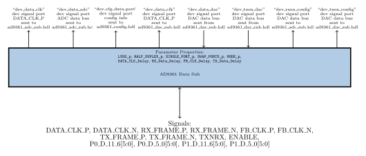
Figure 184: ad9361_data_sub block diagram.
Interface
<HdlDevice language="vhdl"
  ExactParts="
    zynq:xc7z020-1-clg484
    zynq_ise:xc7z020_ise_alias-1-clg484
    zynq_ultra:xczu7ev-2-ffvc1156e
    virtex6:xc6vlx240t-1-ff1156
    stratix4:ep4sgx230k-c2-f40
    artix7:xc7a50t-2-csg325"
  ExcludeTargets="altera modelsim questa"
  Libraries="platform">

  <ComponentSpec nocontrol="true"/>

  <!-- Parameters:  per modes in Table 48 and Table 50 in reference manual and Table 11 in the
       regsiter map reference manual.
       Of course the worker will only be built for valid combinations of parameter values. -->

  <!-- This parameter property corresponds to the "LVDS Mode" bit 4 in the parallel port configuration 3
       register at 0x012. -->
  <Property name='LVDS_p' type='bool' parameter='true' default='false'
            description='Use LVDS mode for Data/clock/frame signals, otherwise use CMOS mode.
			 Default is CMOS/single-ended mode.'/>
  <!-- This parameter property corresponds to the "Half Duplex Mode" bit 3 in the parallel port
       configuration 3 register 0x12 -->
  <Property name='HALF_DUPLEX_p' type='bool' parameter='true' default='false'
            description='Use half duplex mode, otherwise use full duplex mode. Must be false when using LVDS mode.'/>
  <!-- This parameter property corresponds to the "Single Port Mode" bit 2 in the parallel port
       configuration 3 register 0x12 -->
  <Property name='SINGLE_PORT_p' type='bool' parameter='true' default='false'
            description='Use single port, otherwise use both (dual) ports.  Default is to use both ports. Must be false when using LVDS mode.'/>
  <!-- This parameter property corresponds to the "Swap Ports" bit 6 in the parallel port
       configuration 3 register 0x12 -->
  <Property name='SWAP_PORTS_p' type='bool' parameter='true' default='false'
            description='Swaps Port 0 and Port 1. Must be false when using LVDS mode.'/>
  <!-- The MODE_p parameter just maps the above 4 booleans into 8 modes, which determine pin usage
       These modes are listed in the same order as the Digital Interface Specification section and Tables 48 and 50 in the
       reference manual (UG570), with swapped modes inserted.

    modes:                           P0[11:6] P0[5:0] P1[11:6] P1[5:0]
    CMOS:
      0. single port half duplex:    inout    inout   unused   unused
      1. ==same with SwapPorts       unused   unused  inout    inout
      2. single port full duplex:    out      in      unused   unused
      3. ==same with SwapPorts       unused   unused  out      in
      4. dual port half duplex:      inout    inout   inout    inout (swap is the same)
      5. dual port full duplex:      in       in      out      out
      6. ==same with SwapPorts:      out      out     in       in
    LVDS:
      7. dual port full duplex:      out      out     in       in

    So the following expression just encodes the above table for convenience in setting the
    signal direction attributes.  Note mode 6 and 7 have identical signal directions but are
    still used to distinguish enabling LVDS
  -->
  <Property name='MODE_p' type='uchar' parameter='true'
	    default='lvds_p ? 7 :
		     single_port_p ? (half_duplex_p ? (swap_ports_p ? 1 : 0) : (swap_ports_p ? 3 : 2)) :
		     half_duplex_p ? 4 : (swap_ports_p ? 6 : 5)'
            description='a convenience parameter to map the various options into 8 modes.'/>
  <Property name="DATA_CLK_Delay"
            type="ushort"
            parameter="true"
            description="Ushort representation of AD9361 SPI Register 0x006 -
                         DATA_CLK Delay bits. These bits affect the
                         DATA_CLK delay. The typical delay is approximately
                         0.3 ns/LSB. Minimum delay setting is 0x0 and maximum
                         delay setting is 0xF. Set this value so that the
                         data from the AD9361 meets FPGA setup/hold
                         specifications.
                         Because the DATA_CLK delay is specific to a platform or
                         platform/card, the value of this parameter property
                         should be enforced wherever 1) a platform which
                         instantiates this device worker is defined or 2) a
                         platform with a card which instantiates this device
                         worker is defined. There may be future framework
                         features added to better facilitate such enforcement,
                         but currently the only places where this enforcement is
                         possible is in a 1) a platform XML for a platform which
                         instantiates this device worker, 2) a platform
                         configuration for a card which includes this device
                         worker, or 3) a container for a card which includes
                         this device worker."/>
  <Property name="RX_Data_Delay"
            type="ushort"
            parameter="true"
            description="Ushort representation of AD9361 SPI Register 0x006 -
                         RX Data Delay bits. These bits affect the
                         Rx data delay. The typical delay is approximately
                         0.3 ns/LSB. Minimum delay setting is 0x0 and maximum
                         delay setting is 0xF. Set this value so that the
                         data from the AD9361 meets FPGA setup/hold
                         specifications.
                         Because the Rx data delay is specific to a platform or
                         platform/card, the value of this parameter property
                         should be enforced wherever 1) a platform which
                         instantiates this device worker is defined or 2) a
                         platform with a card which instantiates this device
                         worker is defined. There may be future framework
                         features added to better facilitate such enforcement,
                         but currently the only places where this enforcement is
                         possible is in a 1) a platform XML for a platform which
                         instantiates this device worker, 2) a platform
                         configuration for a card which includes this device
                         worker, or 3) a container for a card which includes
                         this device worker."/>

  <Property name="FB_CLK_Delay"
            type="ushort"
            parameter="true"
            description="Ushort representation of AD9361 SPI Register 0x007 -
                         FB_CLK Delay bits. These bits function the same as
                         DATA_CLK and RX data delays but affect the FB_CLK
                         delay. Set this value so that the data from the AD9361
                         meets FPGA setup/hold specifications.
                         Because the FB_CLK delay is specific to a platform or
                         platform/card, the value of this parameter property
                         should be enforced wherever 1) a platform which
                         instantiates this device worker is defined or 2) a
                         platform with a card which instantiates this device
                         worker is defined. There may be future framework
                         features added to better facilitate such enforcement,
                         but currently the only places where this enforcement is
                         possible is in a 1) a platform XML for a platform which
                         instantiates this device worker, 2) a platform
                         configuration for a card which includes this device
                         worker, or 3) a container for a card which includes
                         this device worker."/>
  <Property name="TX_Data_Delay"
            type="ushort"
            parameter="true"
            description="Ushort representation of AD9361 SPI Register 0x007 -
                         TX Data Delay bits. These bits function the same as
                         DATA_CLK and RX data delays but affect the Tx_FRAME and
                         TX Data delay. Tx frame sync is delayed the same amount
                         as the data port bits. Set this value so that the data
                         from the AD9361 meets FPGA setup/hold specifications.
                         Because the Tx_FRAME/TX Data delay is specific to a
                         platform or platform/card, the value of this parameter
                         property should be enforced wherever 1) a platform
                         which instantiates this device worker is defined or 2)
                         a platform with a card which instantiates this device
                         worker is defined. There may be future framework
                         features added to better facilitate such enforcement,
                         but currently the only places where this enforcement is
                         possible is in a 1) a platform XML for a platform which
                         instantiates this device worker, 2) a platform
                         configuration for a card which includes this device
                         worker, or 3) a container for a card which includes
                         this device worker."/>
  <!-- Dev Signal Ports -->
  <devsignal name='dev_cfg_data_port' signals='ad9361-cfg-data-port-signals.xml'/>
  <devsignal name='dev_data_clk' count='3' optional='true' signals='ad9361-data-clk-signals.xml'/>
  <devsignal name='dev_data_adc' optional='true' signals='ad9361-data-adc-signals.xml'/>
  <devsignal name='dev_data_dac' optional='true' signals='ad9361-data-dac-signals.xml'/>
  <!--devsignal name='dev_rxen_adc' optional='true' signals='rxen-out-signals.xml'/--> <!-- TODO / FIXME - support this -->
  <devsignal name='dev_txen_dac' optional='true' signals='txen-out-signals.xml'/>
  <devsignal name='dev_rxen_config' optional='true' signals='rxen-in-signals.xml'/>
  <devsignal name='dev_txen_config' optional='true' signals='txen-in-signals.xml'/>

  <!-- Sub-Device Port Connections (Supports) -->
  <supports worker='ad9361_config'>
    <connect port="dev_cfg_data_port" to="dev_cfg_data_port"/>
    <connect port="dev_rxen_data_sub" to="dev_rxen_config"/>
    <connect port="dev_txen_data_sub" to="dev_txen_config"/>
    <connect port="dev_data_clk" to="dev_data_clk" index='2'/>
  </supports>
  <supports worker='ad9361_adc_sub'>
    <connect port="dev_data_clk" to="dev_data_clk" index='0'/>
    <connect port="dev_data_from_pins" to="dev_data_adc"/>
    <!--connect port="dev_rxen" to="dev_rxen_adc"/--> <!-- TODO / FIXME - support this -->
  </supports>
  <supports worker='ad9361_dac_sub'>
    <connect port="dev_data_clk" to="dev_data_clk" index='1'/>
    <connect port="dev_data_to_pins" to="dev_data_dac"/>
    <connect port="dev_txen" to="dev_txen_dac"/>
  </supports>

  <!-- Signals per data sheet.  Necessary changes from the data sheet signal naming:
       When a differential signal is used in CMOS mode, the positive (e.g. DATA_CLK_P) signal is
       used, but the data sheet may use the signal name without any suffix (e.g. DATA_CLK)
       The two ports (P0_D[11:0] and P1_D [11:0]) are split in half since the halves are in fact
       sometimes used in opposite directions.
       Direction of most signals depends on the mode       ***** NOTE: Because the worker inner layer coded explicitly instances I/O
                   buffer primitives, e.g. BUFFER_IN_1, pin='1' is used below. -->
  <Signal name='DATA_CLK_P' direction='in' pin='1'
	  description='Pin G11: RX Clock from ad9361 (positive).'/>
  <Signal name='DATA_CLK_N' direction='lvds_p ? in : unused' pin='1'
	  description='Pin H11: RX Clock from ad9361 (negative), unused in CMOS mode.'/>
  <Signal name='RX_FRAME_P' direction='in' pin='1'
	  description='Pin G8:  Receive Digital Data Framing Output Signal from ad9361 (positive).'/>
  <Signal name='RX_FRAME_N' direction='lvds_p ? in : unused' pin='1'
	  description='Pin G7:  Receive Digital Data Framing Output Signal from ad9361 (negative), unused in CMOS mode.'/>
  <!-- theoretically these might not be connected in a receive-only configuration -->
  <Signal name='FB_CLK_P'   direction='out' pin='1'
	  description='Pin F10: TX Clock to ad9361 (positive).'/>
  <Signal name='FB_CLK_N'   direction='out' pin='1'
	  description='Pin G10: TX Clock to ad9361 (negative), grounded in CMOS mode.'/>
  <Signal name='TX_FRAME_P' direction='out' pin='1'
	  description='Pin G9:  Transmit Digital Data Framing Input Signal from ad9361 (positive).'/>
  <Signal name='TX_FRAME_N' direction='out' pin='1'
	  description='Pin H9:  Transmit Digital Data Framing Input Signal from ad9361 (negative), grounded in CMOS mode.'/>
  <!-- P0 signals are aliased to LVDS TX_D[5:0]_N and TX_D[5:0]_P pairs in the data sheet -->
  <Signal name='P0_D_11_6' width='6' pin='1' direction='mode_p == 0 || mode_p == 4 ? inout :
		 					mode_p == 1 || mode_p == 3 ? unused :
							mode_p == 5 ? in : out'/>
  <Signal name='P0_D_5_0'  width='6' pin='1' direction='mode_p == 0 || mode_p == 4 ? inout :
							mode_p == 1 || mode_p == 3 ? unused :
							mode_p == 2 || mode_p == 5 ? in :
							out'/>
  <!-- P1 signals are aliased to LVDS RX_D[5:0]_N and RX_D[5:0]_P pairs in the data sheet -->
  <Signal name='P1_D_11_6' width='6' pin='1' direction='mode_p == 0 || mode_p == 2 ? unused :
							mode_p == 1 || mode_p == 4 ? inout :
							mode_p == 6 || mode_p == 7 ? in :
							out'/>
  <Signal name='P1_D_5_0'  width='6' pin='1' direction='mode_p == 0 || mode_p == 2 ? unused :
							mode_p == 1 || mode_p == 4 ? inout :
							mode_p == 5 ? out :
							in'/>
</HdlDevice>
Implementations
ad9361_data_sub(HDL)
Dependencies
The dependencies to other elements in OpenCPI are:
assets/hdl/devices/ad9361_data_sub.hdl/ad9361_data_sub.cpp_vhd
Limitations
Limitations of ad9361_data_sub are:
None.
Testing
Tested platforms include Agilent Zedboard/Analog Devices FMCOMMS2, Agilent Zedboard/Analog Devices FMCOMMS3, Ettus E310 (Vivado only).
The test outlined in Ad9361 dac (ad9361_dac) includes validation of this worker’s functionality (for LVDS mode and CMOS Single Port Full Duplex DDR mode).