Ad9361 config (ad9361_config)
Design
The AD9361 Config is a subdevice worker which provides an entry point to the major functionality of the AD9361 IC. This includes both SPI bus functionality for intercommunication with the AD9361 register map as well as additional command/control between the software and the FPGA. Note that, while the register address decoding is performed within this worker, the SPI state machine itself is implemented in one or more separate, platform-specific or card-specific subdevice workers Ad9361 spi (ad9361_spi). This worker’s register map provides an API for integrating with AD9361 No-OS Software [Analog Devices Wiki]. This integration is implemented in Ad9361 config proxy (ad9361_config_proxy).
A block diagram representation of the implementation is given in Figure 181:
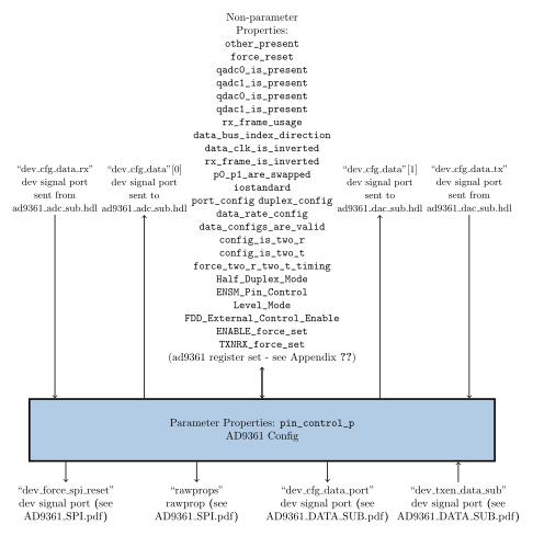
Figure 181: ad9361_config block diagram.
Interface
<!-- ad9361_config.hdl is a device worker containing all functionality necessary
     for AD9361 hardware configuration (register access and pin control). -->
<HdlDevice language="vhdl" FirstRawproperty='general_spi_conf'
  ExactParts="
    zynq:xc7z020-1-clg484
    zynq_ise:xc7z020_ise_alias-1-clg484
    zynq_ultra:xczu7ev-2-ffvc1156e
    virtex6:xc6vlx240t-1-ff1156
    stratix4:ep4sgx230k-c2-f40
    artix7:xc7a50t-2-csg325"
  SourceFiles="signals.vhd"
  Libraries="platform">

  <ControlInterface Timeout="1024"/>

  <!-- By design, this worker provides control and/or data plane functionality
       that is never intended to be exposed by any other worker. Accordingly,
       this worker defines the ComponentSpec element inside this OWD file, as
       opposed to creating an OCS file including said functionality which could
       be used by other workers. -->
  <ComponentSpec>
    <!-- Properties -->
    <!-- Note this is not volatile since it is determined in the container -->
    <property name='other_present'          type='bool'/>

    <property name='force_reset'            type='bool' writable='1' default='0' description='Forces reset pin low (active low). Reset pin is otherwise the same level as the OpenCPI control plane reset signal.'/>
    <!--property name='adc_mode' type='enum' enums='cmos_singleport_halfduplex_sdr,cmos_singleport_halfduplex_ddr,cmos_singleport_fullduplex_sdr,cmos_singleport_fullduplex_ddr,cmos_dualport_halfduplex,cmos_dualport_fullduplex,lvds_dualport_fullduplex,invalid' volatile='1'/-->
    <!--property name='one_t_timing_is_supported' type='bool' volatile='1'/-->
    <property name='qadc0_is_present'       type='bool' volatile='1' description='Inidicates whether or not bitstream was built with qadc0, which supports first RX channel'/>
    <property name='qadc1_is_present'       type='bool' volatile='1' description='Inidicates whether or not bitstream was built with qadc1, which supports second RX channel'/>
    <property name='qdac0_is_present'       type='bool' volatile='1' description='Inidicates whether or not bitstream was built with qdac0, which supports first TX channel'/>
    <property name='qdac1_is_present'       type='bool' volatile='1' description='Inidicates whether or not bitstream was built with qdac1, which supports second TX channel'/>
    <property name='rx_frame_usage'         type='enum' enums='enable,toggle' volatile='1' description='enable : Register 0x010 bit D3 is 0, meaning Rx frame goes high coincident with the first valid receive sample. It stays high., toggle: Register 0x010 bit D3 is 1, meaning the Rx frame signal toggles with a duty cycle of 50%.'/>
    <property name='data_bus_index_direction' type='enum' enums='normal,reverse' volatile='1' description="normal : Register 0x010 bit D1 is 0, meaning each RX sample's bit index direction is normal, i.e. [11:0], reverse: Register 0x010 bit D1 is 1, meaning each RX sample's bit direction is inverted, i.e. [0:11]."/>
    <property name='data_clk_is_inverted'   type='bool' volatile='1' description="false : Register 0x010 bit D0 is 0, meaning that the DATA_CLK follows the DATA_CLK_P signal in the UG570 timing diagrams, true : Register 0x010 bit D0 is 1, meaning that the DATA_CLK follows the DATA_CLK_N signal in the UG570 timing diagrams"/>
    <property name='rx_frame_is_inverted'   type='bool' volatile='1' description="false : Register 0x011 bit D2 is 0, meaning that the RX_FRAME follows the RX_FRAME_P signal in the UG570 timing diagrams, true : Register 0x011 bit D2 is 1, meaning that the RX_FRAME follows the RX_FRAME_N signal in the UG570 timing diagrams"/>
    <property name='LVDS'                   type='bool' volatile='1' description="Value is true if bitstream was built to use LVDS mode for Data/clock/frame signals, and false if CMOS mode was used."/>
    <property name='single_port'            type='bool' volatile='1' description="Value is true if bitstream was built to use single port, and false if dual ports."/>
    <property name='swap_ports'             type='bool' volatile='1' description="Value is true if bitstream was built to swap Port 0 and Port 1, and false if there was no swap."/>
    <property name='half_duplex'            type='bool' volatile='1' description="Value is true if bitstream was built to use half duplex mode, and false if full duplex mode."/>
    <property name='data_rate_config'       type='enum' enums='SDR,DDR'     volatile='1' description="Value indicates which data rate mode (SDR/DDR) the bitstream was built to use."/>
    <property name='data_configs_are_valid' type='bool' volatile='1' description="Value is false if bitstream was built using erroneous combination of LVDS/single port/half duplex/data rate config modes (takes into account build configurations for both ad9361_adc_sub and ad9361_dac_sub workers)."/>
    <property name='config_is_two_r'        type='bool' writable='1' description="Used to tell the ad9361_adc_sub and ad9361_dac_sub workers what data paths are enabled. Note that, just because a qadc or qdac worker is present in the bitstream, that doesn't mean it is enabled."/>
    <property name='config_is_two_t'        type='bool' writable='1' description="Used to tell the ad9361_dac_sub worker what data paths are enabled. Note that, just because a qdac worker is present in the bitstream, that doesn't mean it is enabled."/>
    <property name='force_two_r_two_t_timing' type='bool' writable='1' description="Used to force the ad9361_dac_sub worker to use the 2R2T timing diagram regardless of what TX channels are enabled. This property is expected to correspond to the D2 bit of the Parallel Port Configuration 1 register at SPI address 0x010."/>


    <!-- These properties exists in order to allow this worker to drive the
         AD9361 pin control-related dev signals to their proper value, which is
         dependent upon these registers which these properties are related to.
         Adding these properties was easier than autonomously determining
         register contents inside the worker, which would have necessitated and
        HDL-issued SPI read and bitmasking. -->
    <property name='Half_Duplex_Mode'            type='bool' writable='1' default='false'/>
    <property name='ENSM_Pin_Control'            type='bool' writable='1' default='true'
                                                 description='Intended to match AD9361 register 0x014 bit D4.'/>
    <property name='Level_Mode'                  type='bool' writable='1' default='false'
                                                 description='Intended to match AD9361 register 0x014 bit D3.'/>
    <property name='FDD_External_Control_Enable' type='bool' writable='1' default='false'
                                                 description='Intended to match AD9361 register 0x014 bit D7.'/>

    <!-- These properties exists in order to allow for use of FDD independent
         mode, which requires forcing this pin values prior to setting the ENSM
         into the FDD independent state (vs. having them driven
         by e.g. qdac event port(s), which is the default behavior once in the
         FDD independent state) -->
    <property name='ENABLE_force_set' type='bool' writable='1' default='false'
                                      description='Forces set of AD9361 ENABLE pin'/>
    <property name='TXNRX_force_set' type='bool' writable='1' default='false'
                                     description='Forces set of AD9361 TXNRX pin'/>

    <!-- Here are the raw properties that are in registers -->
    <include href='ad9361-properties'/>
  </ComponentSpec>

  <!-- Parameter Properties -->
  <property name='pin_control_p' type='bool'
                                 parameter='true'
                                 description='
      Whether RX/TX powerdown via pin control is possible.'/>

  <!-- Raw Property Ports -->
  <rawprop name='rawprops' master='true'/>

  <!-- Dev Signal Ports -->
  <devsignal name='dev_force_spi_reset' signals='force-reset-out-signals.xml'      master='true'/>
  <devsignal name='dev_cfg_data_port'   signals='ad9361-cfg-data-port-signals.xml' master='true'/>
  <devsignal name='dev_cfg_data' count='2' optional='true' signals='ad9361-cfg-data-signals.xml'/>
  <devsignal name='dev_cfg_data_rx'        optional='true' signals='ad9361-cfg-data-rx-signals.xml'/>
  <devsignal name='dev_cfg_data_tx'        optional='true' signals='ad9361-cfg-data-tx-signals.xml'/>
  <devsignal name='dev_rxen_data_sub'   signals='rxen-in-signals.xml' master='true'/>
  <devsignal name='dev_txen_data_sub'   signals='txen-in-signals.xml' master='true'/>
  <devsignal name='dev_data_clk'        signals='ad9361-data-clk-signals.xml'      master='true'/>

  <!-- Sub-Device Port Connections (Supports) -->
  <supports worker='ad9361_adc_sub'>
    <connect port="dev_cfg_data"    to="dev_cfg_data" index='0'/>
    <connect port="dev_cfg_data_rx" to="dev_cfg_data_rx"/>
  </supports>

  <supports worker='ad9361_dac_sub'>
    <connect port="dev_cfg_data"    to="dev_cfg_data" index='1'/>
    <connect port="dev_cfg_data_tx" to="dev_cfg_data_tx"/>
  </supports>

  <!-- Signals -->
  <signal name="ENABLE" direction="out"
                        description="Control Input. This pin moves the devices
                                     through various operational states"/>
  <signal name="TXNRX" direction="out"
                       description="Enable State Machine Control Signal."/>

</HdlDevice>
Implementations
ad9361_config(HDL)
Dependencies
The dependencies to other elements in OpenCPI are:
assets/hdl/devices/ad9361_config.hdl/ad9361_config.vhd
assets/hdl/devices/ad9361_config.hdl/signals.vhd
Limitations
Limitations of ad9361_config are:
None.
Testing
Tested platforms include Agilent Zedboard/Analog Devices FMCOMMS2 (Vivado only), Agilent Zedboard/Analog Devices FMCOMMS3 (Vivado only), Ettus E310 (Vivado only).
No standalone unit test currently exists for this worker. However, the test outlined in Ad9361 dac (ad9361_dac) includes validation of a subset of this worker’s functionality (for LVDS only).
Appendix
The full ad9361_config.hdl register-map property table is documented in Appendix - ad9361_config.hdl Properties, and the Vivado timing analysis for this worker is documented in Appendix - Vivado Timing Analysis.